Faster, ultra reliable, and ultra energy-efficient graphene interconnects
Semiconductor industry’s very first CMOS-compatible, low-temperature, 300mm-scale, graphene interconnect technology

State-of-the-art interconnect material copper (Cu) is running out of steam due to a non-linear increase in resistivity with scaling, which degrades performance, reliability, and energy-efficiency. The semiconductor industry is actively looking for a solution.
Engineered graphene offers lower resistivity and up to 100-folds higher current-carrying capacity, compared to conventional Cu interconnects, leading to faster, more reliable, thinner, and more energy-efficient interconnects.
For CMOS and related microelectronics applications, high-quality graphene must be directly deposited (transfer-free) on a variety of substrates including dielectrics and metal layers at back-end-of-line (BEOL) compatible temperatures (<450 °C), which makes conventional graphene growth via chemical vapor deposition and other methods unsuitable since they require significantly higher temperatures.
More information on interconnect scaling and graphene synthesis challenges can be found here
")

Multi-layer Graphene (MLG)
MLG Interconnects

Destination 2D graphene can be directly synthesized on various substrates at BEOL- compatible temperatures through our innovative process technology and proprietary 300mm synthesis tool CoolC™.
CoolC™

- Industry first
- 300mm graphene synthesis equipment
- Transfer free – direct synthesis
- BEOL compatible low temperature process
- Industry standard interfaces
- Green
Other Applications
In addition to the transformative changes we envision by introducing a revolutionary interconnect technology paradigm for CMOS logic and memory, our CMOS-compatible graphene technology can also provide unique and smart solutions for:

Transparent Electrodes for Solar Cells

EUV Mask Pellicles
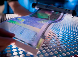
Flexible Displays & Touch Panels
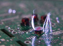
Electrostatic Discharge (ESD) Protection
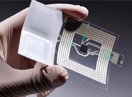
Printed Batteries